An atomic array in silicon paves the way for large scale devices
A University of Melbourne led team have perfected a technique for embedding single atoms in a silicon wafer one-by-one. Their technology offers the potential to make quantum computers using the same methods that have given us cheap and reliable conventional devices containing billions of transistors.
“We could ‘hear’ the electronic click as each atom dropped into one of 10,000 sites in our prototype device. Our vision is to use this technique to build a very, very large-scale quantum device,” says Professor David Jamieson of The University of Melbourne, lead author of the Advanced Materials paper describing the process.

His co-authors are from UNSW Sydney, Helmholtz-Zentrum Dresden-Rossendorf (HZDR), Leibniz Institute of Surface Engineering (IOM), and RMIT Microscopy and Microanalysis Facility.
“We believe we ultimately could make large-scale machines based on single atom quantum bits by using our method and taking advantage of the manufacturing techniques that the semiconductor industry has perfected,” he says.
Until now, implanting atoms in silicon has been a haphazard process, where a silicon chip gets showered with phosphorus which implant in a random pattern, like raindrops on a window.
“We embedded phosphorus ions, precisely counting each one, in a silicon substrate creating a qubit ‘chip’, which can then be used in lab experiments to test designs for large scale devices.”
“This will allow us to engineer the quantum logic operations between large arrays of individual atoms, retaining highly accurate operations across the whole processor,” says UNSW’s Scientia Professor Andrea Morello, a joint author of the paper. “Instead of implanting many atoms in random locations and selecting the ones that work best, they will now be placed in an orderly array, similar to the transistors in conventional semiconductors computer chips.”
“We used advanced technology developed for sensitive x-ray detectors and a special atomic force microscope originally developed for the Rosetta space mission along with a comprehensive computer model for the trajectory of ions implanted into silicon, developed in collaboration with our colleagues in Germany,” says Dr Alexander (Melvin) Jakob, first author of the paper, also from the University of Melbourne.
This new technique can create large scale patterns of counted atoms that are controlled so their quantum states can be manipulated, coupled and read-out.
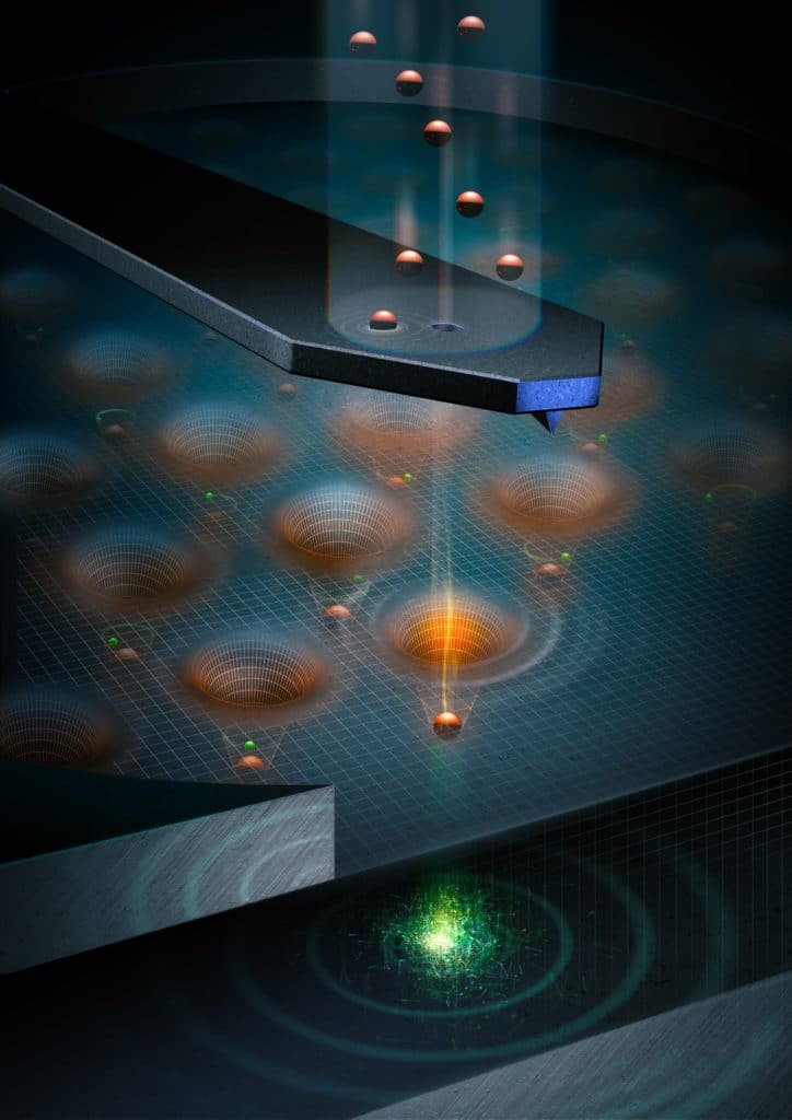
The technique developed by Professor Jamieson and his colleagues takes advantage of the precision of the atomic force microscope, which has a sharp cantilever that gently ‘touches’ the surface of a chip with a positioning accuracy of just half a nanometre, about the same as the spacing between atoms in a silicon crystal.
The team drilled a tiny hole in this cantilever, so that when it was showered with phosphorus atoms one would occasionally drop through the hole and embed in the silicon substrate.
The key, however, was knowing precisely when one atom – and no more than one – had become embedded in the substrate. Then the cantilever could move to the next precise position on the array.
The team discovered that the kinetic energy of the atom as it ploughs into the silicon crystal and dissipates its energy by friction can be exploited to make a tiny electronic ‘click’.
That is how they know an atom has embedded in the silicon and to move to the next precise position.
“One atom colliding with a piece of silicon makes a very faint click, but we have invented very sensitive electronics used to detect the click, it’s much amplified and gives a loud signal, a loud and reliable signal,” says Professor Jamieson.
“That allows us to be very confident of our method. We can say, ’Oh, there was a click. An atom just arrived’. Now we can move the cantilever to the next spot and wait for the next atom.”
“With our Centre partners, we have already produced ground-breaking results on single atom qubits made with this technique, but the new discovery will accelerate our work on large-scale devices,” he says.
The project was funded by the Australian Research Council Centre of Excellence for Quantum Computation and Communication Technology (CQC²T) and the US Army Research Office, a grant from The University of Melbourne Research and Infrastructure Fund (RIF) and use of the facilities of the Australian National Fabrication Facility (ANFF) at the Melbourne Centre for Nanofabrication (MCN).

